Introduction
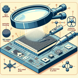
In the world of nanotechnology, achieving precision in nanopatterning is paramount for the development of nanoelectronic devices and high-density recording systems. Traditional methods like optical and electron beam lithography are often expensive and complex. However, the study titled "Nanopatterning on silicon surface using atomic force microscopy with diamond-like carbon (DLC)-coated Si probe" introduces an innovative approach using Atomic Force Microscopy (AFM) equipped with a DLC-coated Si probe. This method promises a cost-effective and efficient alternative for nanofabrication on hard surfaces like silicon.
Key Findings
The research highlights several crucial aspects of using a DLC-coated Si probe for scratch nanolithography:
- Scratch Direction: The direction of the scratch significantly impacts the depth and precision of the grooves. Forward scratching with a sharp cutting edge results in deeper grooves compared to backward scratching.
- Applied Tip Force: The size of the grooves increases with the applied tip force. In the low-force regime (1-10 µN), the groove depth and width increase linearly, while in the high-force regime (12-20 µN), the increase slows down, indicating saturation.
- Scratch Speed: While the depth of the grooves remains relatively constant with varying speeds, the width decreases significantly at lower speeds and stabilizes at higher speeds.
- Number of Scratches: Repeated scratching along the same path can enlarge the groove size, with both depth and width increasing linearly with the number of scratches.
Implications for Practitioners
For practitioners in the field of nanotechnology, the findings of this research offer a practical and economical approach to nanopatterning:
- Cost-Effectiveness: The use of DLC-coated probes is significantly cheaper than diamond-coated alternatives, making it accessible for broader applications.
- Precision and Control: The ability to control scratch parameters such as direction, force, and speed allows for precise fabrication of complex nanostructures.
- Scalability: This method can potentially be scaled for large-scale nanofabrication, enhancing its applicability in industrial settings.
Encouragement for Further Research
While this study provides a solid foundation, further research is encouraged to explore the full potential of DLC-coated probes in various applications. Investigating different materials and substrates, as well as optimizing scratch parameters, could lead to even more efficient and precise nanofabrication techniques.
To read the original research paper, please follow this link: Nanopatterning on silicon surface using atomic force microscopy with diamond-like carbon (DLC)-coated Si probe.